SYSTRAN CORPORATION
SCRAMNET+ REHOSTABLE ADAPTER EVALUATION BOARD
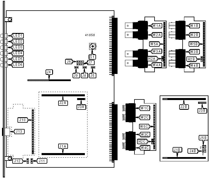
|
NIC Type |
Proprietary |
|
Chipset |
Systran Corporation |
|
Maximum Onboard Memory |
2MB DRAM (on daughterboard) |
|
I/O Options |
Bypass connector |
|
Network Transfer Rate |
150Mbps |
|
Data Bus |
VME double |
|
Topology |
Linear Bus/Ring |
|
Wire Type |
RG-58A/U 50ohm coaxial Fiber optic cable |
|
Boot ROM |
Not available |
|
CONNECTIONS | |||
|
Function |
Label |
Function |
Label |
|
Header to daughterboard J1B |
J1A |
Testing pins |
J7 |
|
Header to main board J1A |
J1B |
Media board header |
J10 |
|
Header to daughterboard J2B |
J2A |
Bypass connector |
J13 |
|
Header to main board J2A |
J2B |
RG-58A/U 50ohm coaxial receive connector 1 |
W1A |
|
Header to daughterboard J3B |
J3A |
Fiber optic ST receive connector 1 |
W1B |
|
Header to main board J3A |
J3B |
Fiber optic SC receive connector 1 |
W1C |
|
Unidentified |
J4 |
RG-58A/U 50ohm coaxial receive connector 2 |
W2A |
|
Testing pins |
J6 |
Fiber optic ST receive connector 2 |
W2B |
|
Fiber optic SC receive connector 2 |
W2C |
Fiber optic ST transmit connector 2 |
W4B |
|
RG-58A/U 50ohm coaxial transmit connector 1 |
W3A |
Fiber optic SC transmit connector 2 |
W4C |
|
Fiber optic ST transmit connector 1 |
W3B |
Header to main board J10 |
W5A |
|
Fiber optic SC transmit connector 1 |
W3C |
Header to main board J10 |
W5B |
|
RG-58A/U 50ohm coaxial transmit connector 2 |
W4A |
Header to main board J10 |
W5C |
|
USER CONFIGURABLE SETTINGS | |||
|
Setting |
Label |
Position | |
| » |
Media card power source is internal |
H2A |
Pins 1 & 2 closed |
|
Media card power source is external |
H2A |
Pins 2 & 3 closed | |
| » |
Media card power source is internal |
H2B |
Pins 1 & 2 closed |
|
Media card power source is external |
H2B |
Pins 2 & 3 closed | |
|
EEPROM write protect disabled |
J4B |
Pins 3 & 4 closed | |
|
EEPROM write protect enabled |
J4B |
Pins 1 & 2 closed | |
| » |
Address bits for internal CSR enabled |
J5 |
Closed |
|
Address bits for internal CSR disabled |
J5 |
Open | |
|
EEPROM read protect disabled |
J5B |
Pins 3 & 4 closed | |
|
EEPROM read protect enabled |
J5B |
Pins 1 & 2 closed | |
| » |
Address bits for memory enabled |
J8 |
Closed |
|
Address bits for memory disabled |
J8 |
Open | |
| » |
Address bits for external CSR enabled |
J9 |
Closed |
|
Address bits for external CSR disabled |
J9 |
Open | |
| » |
TRIG1/TRIG2 |
J11 |
Unidentified |
|
Chassis ground connected to signal ground |
J12 |
Pins 3 & 4 closed | |
|
Chassis ground not connected to signal ground |
J12 |
Pins 1 & 2 closed | |
|
DRAM CONFIGURATION |
|
512KB, 1MB, or 2MB of memory may be factory installed on the daughterboard. The circuitry supports up to 8MB of memory. For other memory configurations, the user must provide an external memory interface. |
|
CSR ADDRESS SELECTION | ||
|
Setting |
S1 | |
| » |
00h, 20h |
Position 0 |
|
40h, 60h |
Position 4 | |
|
80h, 80h |
Position 8 | |
|
C0h, E0h |
Position C | |
|
DIAGNOSTIC LED(S) | |||
|
LED |
Color |
Status |
Condition |
|
LED1 |
Green |
On |
Network connection is good |
|
LED1 |
Green |
Off |
Network connection is broken |
|
LED2 |
Green |
On |
Message is waiting in transmit FIFO |
|
LED2 |
Green |
Off |
Message is not waiting in transmit FIFO |
|
LED3 |
Green |
On |
Carrier signal is detected |
|
LED3 |
Green |
Off |
Carrier signal is not detected |
|
LED4 |
Yellow |
On |
Error condition detected |
|
LED4 |
Yellow |
Off |
Error condition not detected |
|
LED5 |
Green |
On |
Message received from this node |
|
LED5 |
Green |
Off |
Message not received from this node |
|
LED6 |
Green |
On |
Message received from another node |
|
LED6 |
Green |
Off |
Message not received from another node |
|
MISCELLANEOUS TECHNICAL NOTE |
|
The daughterboard is designed as a prototyping card for the user to design a VME bus network interface around. The main board shown above is only an evaluation board and is a separate product. |