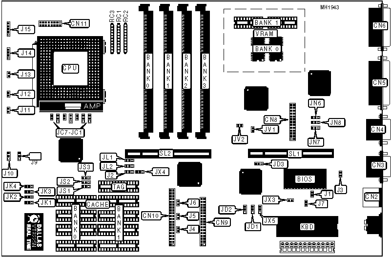
FIRST INTERNATIONAL COMPUTER, INC.
486-GAC-V
|
Processor |
80486SX/CX486S/SL enhanced/80486DX 80486DX2/80486DX4/Pentium Overdrive |
|
Processor Speed |
25/33/40/50(internal)/66(internal)/100(internal)MHz |
|
Chip Set |
VIA |
|
Max. Onboard DRAM |
64MB |
|
Cache |
64/128/256KB |
|
BIOS |
Award |
|
Dimensions |
330mm x 218mm |
|
I/O Options |
3.3V Daughter board connector, 32-bit VESA local bus slot, floppy drive interface,IDE interface, parallel port, PS/2 mouse port, serial ports (2), VGA feature connector, VGA port |
|
NPU Options |
None |
|
CONNECTIONS | |||
|
Purpose |
Location |
Purpose |
Location |
|
PS/2 keyboard connector |
CN1 |
Green power supply connector |
J3 |
|
PS/2 mouse connector |
CN2 |
IDE interface LED |
J6 |
|
Serial port 1 |
CN3 |
Turbo switch |
J11 |
|
Serial port 2 |
CN4 |
Turbo LED |
J12 |
|
Parallel port |
CN5 |
Reset switch |
J13 |
|
VGA port |
CN6 |
Speaker |
J14 |
|
Video feature connector (8514A) |
CN8 |
Power LED & keylock |
J15 |
|
Floppy drive interface |
CN9 |
ISA Bus slot |
SL1 |
|
IDE interface |
CN10 |
32-bit VESA Local bus slot |
SL2 |
|
3.3V Daughter board connector |
CN11 | ||
|
USER CONFIGURABLE SETTINGS | |||
|
Function |
Jumper |
Position | |
|
» |
I/O Channel not set to Adaptec (transfer rate < 5.7 MB/s) |
J1 |
Open |
|
I/O Channel set to Adaptec ISA Master (1542B/C SCSI) |
J1 |
Closed | |
|
» |
IDE not connected to BALE signal |
J4 |
Open |
|
IDE connected to BALE signal |
J4 |
Closed | |
|
» |
IDE not connected to IOCHRDY signal |
J5 |
Open |
|
IDE connected to IOCHRDY signal |
J5 |
Closed | |
|
» |
Password enabled |
J7 |
Open |
|
Password clear |
J7 |
Closed | |
|
» |
Factory configured do not alter |
J9 |
pins 1 & 2 closed |
|
Pentium Overdrive write-back |
JC7 |
Closed | |
|
Pentium Overdrive write-through |
JC7 |
Open | |
|
» |
Local IDE enabled |
JD3 |
pins 2 & 3 closed |
|
Local IDE disabled |
JD3 |
pins 1 & 2 closed | |
|
» |
NS87312 I/O port address - index port 26eh, data port 26Fh |
JN6 |
pins 1 & 2 closed |
|
NS87312 I/O port address - index port 398h, data port 399h |
JN6 |
pins 2 & 3 closed | |
|
» |
IRQ9 disabled |
JV1 |
Open |
|
IRQ9 enabled |
JV1 |
Closed | |
|
» |
Onboard VGA enabled |
JV2 |
pins 2 & 3 closed |
|
Onboard VGA disabled |
JV2 |
pins 1 & 2 closed | |
|
DRAM CONFIGURATION | ||||
|
Size |
Bank 0 |
Bank 1 |
Bank 2 |
Bank 3 |
|
1MB |
(1) 256K x 36 |
NONE |
NONE |
NONE |
|
2MB |
(1) 256K x 36 |
(1) 256K x 36 |
NONE |
NONE |
|
3MB |
(1) 256K x 36 |
(1) 256K x 36 |
(1) 256K x 36 |
NONE |
|
4MB |
(1) 256K x 36 |
(1) 256K x 36 |
(1) 256K x 36 |
(1) 256K x 36 |
|
4MB |
(1) 1M x 36 |
NONE |
NONE |
NONE |
|
5MB |
(1) 1M x 36 |
(1) 256K x 36 |
NONE |
NONE |
|
6MB |
(1) 1M x 36 |
(1) 256K x 36 |
(1) 256K x 36 |
NONE |
|
7MB |
(1) 1M x 36 |
(1) 256K x 36 |
(1) 256K x 36 |
(1) 256K x 36 |
|
8MB |
(1) 1M x 36 |
(1) 1M x 36 |
NONE |
NONE |
|
12MB |
(1) 1M x 36 |
(1) 1M x 36 |
(1) 1M x 36 |
NONE |
|
12MB |
NONE |
(1) 1M x 36 |
(1) 2M x 36 |
NONE |
|
12MB |
NONE |
NONE |
(1) 1M x 36 |
(1) 2M x 36 |
|
16MB |
(1) 1M x 36 |
(1) 1M x 36 |
(1) 1M x 36 |
(1) 1M x 36 |
|
16MB |
(1) 4M x 36 |
NONE |
NONE |
NONE |
|
16MB |
NONE |
(1) 1M x 36 |
(1) 2M x 36 |
(1) 1M x 36 |
|
16MB |
NONE |
NONE |
(1) 2M x 36 |
(1) 2M x 36 |
|
17MB |
(1) 4M x 36 |
(1) 256K x 36 |
NONE |
NONE |
|
18MB |
(1) 4M x 36 |
(1) 256K x 36 |
(1) 256K x 36 |
NONE |
|
19MB |
(1) 4M x 36 |
(1) 256K x 36 |
(1) 256K x 36 |
(1) 256K x 36 |
|
20MB |
(1) 4M x 36 |
(1) 1M x 36 |
NONE |
NONE |
|
21MB |
(1) 4M x 36 |
(1) 1M x 36 |
(1) 256K x 36 |
NONE |
|
22MB |
(1) 4M x 36 |
(1) 1M x 36 |
(1) 256K x 36 |
(1) 256K x 36 |
|
24MB |
(1) 4M x 36 |
(1) 1M x 36 |
(1) 1M x 36 |
NONE |
|
28MB |
(1) 4M x 36 |
(1) 1M x 36 |
(1) 1M x 36 |
(1) 1M x 36 |
|
32MB |
(1) 4M x 36 |
(1) 4M x 36 |
NONE |
NONE |
|
32MB |
NONE |
NONE |
(1) 8M x 36 |
NONE |
|
32MB |
NONE |
NONE |
NONE |
(1) 8M x 36 |
|
33MB |
(1) 4M x 36 |
(1) 4M x 36 |
(1) 256K x 36 |
NONE |
|
34MB |
(1) 4M x 36 |
(1) 4M x 36 |
(1) 256K x 36 |
(1) 256K x 36 |
|
36MB |
(1) 4M x 36 |
(1) 4M x 36 |
(1) 1M x 36 |
NONE |
|
40MB |
(1) 4M x 36 |
(1) 4M x 36 |
(1) 1M x 36 |
(1) 1M x 36 |
|
48MB |
(1) 4M x 36 |
(1) 4M x 36 |
(1) 4M x 36 |
NONE |
|
48MB |
NONE |
(1) 4M x 36 |
(1) 8M x 36 |
NONE |
|
48MB |
NONE |
NONE |
(1) 4M x 36 |
(1) 8M x 36 |
|
64MB |
(1) 4M x 36 |
(1) 4M x 36 |
(1) 4M x 36 |
(1) 4M x 36 |
|
CACHE CONFIGURATION | |||
|
Size |
Bank 0 |
Bank 1 |
TAG (M9) |
|
64KB |
(4) 8K x 8 |
(4) 8K x 8 |
(1) 8K x 8 |
|
128KB |
(4) 32K x 8 |
NONE |
(1) 8K x 8 |
|
256KB |
(4) 32K x 8 |
(4) 32K x 8 |
(1) 32K x 8 |
|
CACHE JUMPER CONFIGURATION | |||
|
Size |
JS1 |
JS2 |
JS3 |
|
64KB |
pins 1 & 2 closed |
pins 1 & 2 closed |
pins 1 & 2 closed |
|
128KB |
pins 2 & 3 closed |
pins 1 & 2 closed |
pins 1 & 2 closed |
|
256KB |
pins 2 & 3 closed |
pins 2 & 3 closed |
pins 2 & 3 closed |
|
VESA WAIT STATE/BUS SPEED CONFIGURATION | |||
|
CPU speed |
Wait states |
JL1 |
JL2 |
|
< 33MHz |
0 wait states |
pins 1 & 2 closed |
pins 1 & 2 closed |
|
> 33MHz |
1 wait state |
pins 2 & 3 closed |
pins 2 & 3 closed |
|
CPU TYPE CONFIGURATION | ||||
|
Type |
JC1 |
JC2 |
JC3 |
JC4 |
|
80486SX |
pins 2 & 3 closed |
pins 2 & 3 closed |
Open |
pins 1 & 2 closed |
|
Cx486S |
pins 2 & 3 closed |
pins 2 & 3 closed |
Open |
pins 1 & 2 closed |
|
Cx487S |
pins 1 & 2 closed |
pins 1 & 2 closed |
Open |
pins 1 & 2 closed |
|
Cx486DX |
pins 1 & 2 closed |
pins 1 & 2 closed |
Open |
pins 1 & 2 closed |
|
AM486DXL |
pins 1 & 2 closed |
pins 1 & 2 closed |
Open |
pins 1 & 2 closed |
|
80486DX |
pins 1 & 2 closed |
pins 1 & 2 closed |
Open |
pins 1 & 2 closed |
|
80486DX2 |
pins 1 & 2 closed |
pins 1 & 2 closed |
Open |
pins 1 & 2 closed |
|
80486DX4 |
pins 1 & 2 closed |
pins 1 & 2 closed |
Open |
pins 1 & 2 closed |
|
Pentium Overdrive |
pins 1 & 2 closed |
pins 1 & 2 closed |
Closed |
pins 2 & 3 closed |
|
CPU TYPE CONFIGURATION (CONTINUED) | ||||
|
Type |
JC5 |
RC1 |
RC2 |
RC3 |
|
80486SX |
Open |
Not Installed |
Not Installed |
Not Installed |
|
Cx486S |
Open |
Not Installed |
Installed |
Not Installed |
|
Cx486DX |
Open |
Not Installed |
Installed |
Not Installed |
|
AM486DXL |
Open |
Not Installed |
Not Installed |
Installed |
|
80486DX |
Open |
Not Installed |
Not Installed |
Not Installed |
|
80486DX2 |
Open |
Not Installed |
Not Installed |
Not Installed |
|
80486DX4 |
Closed |
Installed |
Not Installed |
Not Installed |
|
CPU TYPE CONFIGURATION (CONTINUED) | |||||
|
Type |
J2 |
J10 |
JX3 |
JX4 |
JX5 |
|
Regular CPU |
pins 1 & 2 |
pins 1 & 2 |
N/A |
Open |
pins 1 & 2 |
|
SL-enhanced |
pins 2 & 3 |
pins 2 & 3 |
pins 1 & 2 |
pins 1 & 2 |
pins 2 & 3 |
|
Cyrix CPU |
N/A |
N/A |
pins 2 & 3 |
pins 2 & 3 |
N/A |
|
Note:JX3 may not be available on some mainboards. | |||||
|
Pins designated are in the closed position. | |||||
|
CPU SPEED (VT8225N) CONFIGURATION | ||||
|
Clock |
JK1 |
JK2 |
JK3 |
JK4 |
|
25 MHz |
pins 2 & 3 closed |
pins 1 & 2 closed |
pins 2 & 3 closed |
pins 1 & 2 closed |
|
33 MHz |
pins 2 & 3 closed |
pins 2 & 3 closed |
pins 1 & 2 closed |
pins 1 & 2 closed |
|
40 MHz |
pins 1 & 2 closed |
pins 1 & 2 closed |
pins 2 & 3 closed |
pins 1 & 2 closed |
|
50iMHz |
pins 2 & 3 closed |
pins 1 & 2 closed |
pins 2 & 3 closed |
pins 1 & 2 closed |
|
50 MHz |
pins 2 & 3 closed |
pins 1 & 2 closed |
pins 2 & 3 closed |
pins 2 & 3 closed |
|
66iMHz |
pins 2 & 3 closed |
pins 2 & 3 closed |
pins 1 & 2 closed |
pins 1 & 2 closed |
|
DX4 INTERNAL CLOCK CONFIGURATION | ||
|
Speed |
JC6 | |
| » |
Internal 3 X |
Open |
|
Internal 2.5 X |
pins 1 & 2 closed | |
|
Internal 2 X |
pins 2 & 3 closed | |
|
IDE SPEED SELECT CONFIGURATION (PDC 20230 ONLY) | |||
|
IDE Type |
JD1 |
JD2 | |
| » |
Normal |
pins 2 & 3 closed |
pins 2 & 3 closed |
|
Fast |
pins 1 & 2 closed |
pins 1 & 2 closed | |
|
Medium |
pins 2 & 3 closed |
pins 1 & 2 closed | |
|
PRINTER PORT DIRECTION CONFIGURATION | |||
|
Direction |
JN7 |
JN8 | |
| » |
Output only |
pins 1 & 2 closed |
pins 2 & 3 closed |
|
Input only |
pins 1 & 2 closed |
pins 1 & 2 closed | |
|
Bi-directional |
pins 2 & 3 closed |
Closed | |
|
VRAM CONFIGURATION | ||
|
Size |
Bank 0 |
Bank 1 |
|
1MB |
(2) 512K x 4 |
NONE |
|
2MB |
(2) 512K x 4 |
(2) 512K x 4 |