AXIOM TECHNOLOGY, INC.
SBC8251
|
Processor |
Cyrix/Pentium |
|
Processor Speed |
75/90/100/120/133/150/166/180/200MHz |
|
Chip Set |
Intel |
|
Video Chip Set |
Chips and Technology |
|
Maximum Onboard Memory |
64MB |
|
Maximum Video Memory |
2MB |
|
Cache |
256/512KB |
|
BIOS |
Unidentified |
|
Dimensions |
185mm x 122mm |
|
I/O Options |
Floppy drive interface, IDE interface, parallel port, PS/2 mouse port, PS/2 mouse interface, serial ports (2), VGA port, PC/104 connectors (2) |
|
NPU Options |
None |
|
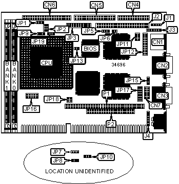
CONNECTIONS | |||
|
Purpose |
Location |
Purpose |
Location |
|
PS/2 mouse port |
CN1 |
Internal buzzer |
JP12/pins 1- 3 |
|
VGA port |
CN2 |
Power LED & keylock |
JP12/pins 2 - 10 |
|
Serial port 1 |
CN3 |
External speaker |
JP12/pins 4 - 7 |
|
Parallel port |
CN4 |
Green PC connector |
JP12/pins 5 & 9 |
|
Floppy drive interface |
CN5 |
Reset switch |
JP12/pins 11 & 12 |
|
IDE interface |
CN6 |
IDE interface LED |
JP12/pins 17 & 18 |
|
Serial port 2 |
CN7 |
Watchdog timer |
JP3/pins 19 & 20 |
|
Power connector |
J1 |
PC/104 connector |
P1 |
|
Power connector |
J3 |
PC/104 connector |
P2 |
|
Keyboard, PS/2 mouse |
J4 | ||
|
USER CONFIGURABLE SETTINGS | |||
|
Function |
Label |
Position | |
|
» |
Factory configured - do not alter |
J2 |
Unidentified |
|
» |
SHFCLK normal operation |
JP5 |
Pins 2 & 3 closed |
|
SHFCLK inverted |
JP5 |
Pins 1 & 2 closed | |
|
Flash BIOS write protect disabled |
JP7 |
Pins 1 & 2 closed | |
|
Flash BIOS write protect enabled |
JP7 |
Pins 2 & 3 closed | |
|
» |
CMOS memory normal operation |
JP8 |
Pins 2 & 3 closed |
|
CMOS memory clear |
JP8 |
Pins 1 & 2 closed | |
|
Cache type select write back |
JP10 |
Pins 2 & 3 closed | |
|
Cache type select write through |
JP10 |
Pins 1 & 2 closed | |
|
System clock = PCI clock/4 |
JP13 |
Open | |
|
System clock = PCI clock/3 |
JP13 |
Closed | |
|
SIMM CONFIGURATION | |
|
Size |
Bank 0 |
|
8MB |
(2) 1M x 36 |
|
16MB |
(2) 2M x 36 |
|
32MB |
(2) 4M x 36 |
|
64MB |
(2) 8M x 36 |
|
SIMM REFRESH RATE CONFIGURATION | |
|
Setting |
JP16/pins 1 & 2 |
|
60MHz |
Closed |
|
66MHz |
Open |
|
CACHE CONFIGURATION |
|
Note: The location of the cache is unidentified. |
|
CACHE JUMPER CONFIGURATION | |
|
Size |
JP16 |
|
256KB |
Pins 3 & 4 closed |
|
512KB |
Pins 5 & 6 closed |
|
VIDEO MEMORY CONFIGURATION |
|
Note: The location of the video memory is unidentified. |
|
CPU BUS SPEED SELECTION | |
|
Speed |
JP18 |
|
50MHz |
Pins 1 & 2, 3 & 4 closed |
|
55MHz |
Open |
|
60MHz |
Pins 3 & 4 closed |
|
66MHz |
Pins 1 & 2 closed |
|
CPU BUS/CORE SELECTION | |
|
Bus/Core |
JP16 |
|
2/5 |
Pins 7 & 8, 9 & 10 closed |
|
1/3 |
Pins 9 & 10 closed |
|
1/2 |
Pins 7 & 8closed |
|
2/3 |
Open |
|
CPU TYPE SELECTION | |
|
Type |
JP9 |
|
Cyrix |
Pins 1 & 2 closed |
|
Intel |
Pins 2 & 3 closed |
|
CPU VOLTAGE SELECTION (SINGLE) | |
|
Voltage |
JP1 |
|
3.3v |
Pins 1 & 2 closed |
|
3.6v |
Pins 2 & 3 closed |
|
CPU VOLTAGE SELECTION (DUAL) | |
|
Voltage |
JP2 |
|
2.7v |
Pins 4 & 6 closed |
|
2.9v |
Pins 2 & 4 closed |
|
3.3v |
Pins 1 & 3 closed |
|
3.45v |
Pins 3 & 5 closed |
|
SERIAL PORT 2 SELECTION | ||
|
Setting |
JP11 |
JP17 |
|
RS232 |
5 & 6 |
3 & 5, 4 & 6, 9 & 11, 10 & 12 |
|
RS422 |
3 & 4 |
1 & 3, 2 & 4, 7 & 9, 8 & 10 |
|
RS485 |
1 & 2 |
1 & 3, 2 & 4, 7 & 9, 8 & 10 |
|
Note: Pins designated should be in the closed position. | ||
|
LCD PANEL INTERFACE SELECTION | ||
|
Setting |
JP6 |
JP15 |
|
3.3v panel |
Closed |
Pins 1 & 2 closed |
|
5v panel |
Open |
Pins 2 & 3 closed |
|
LCD PANEL TYPE SELECTION |
|
Note: Pins 9 & 10, 11 & 12, 13 & 14, 15 & 16 on JP3 are used to select up to 16 typed of LED BIOS. |
|
DISK ON CHIP ADDRESS SELECTION | |
|
Setting |
JP3 |
|
C0000 – C7FFF |
Pins 1 & 2 closed |
|
C8000 – CFFFF |
Pins 3 & 4 closed |
|
D0000 – D7FFF |
Pins 5 & 6 closed |
|
D8000 – DFFFF |
Pins 7 & 8 closed |