ASUS COMPUTER INTERNATIONAL
P/I-P55TP4XEG (VER. 2.4)
|
Processor |
Pentium |
|
Processor Speed |
75/90/100/120/133/150/166MHz |
|
Chip Set |
Intel |
|
Video Chip Set |
None |
|
Maximum Onboard Memory |
128MB (EDO supported) |
|
Maximum Video Memory |
None |
|
Cache |
256/512KB |
|
BIOS |
Award |
|
Dimensions |
330mm x 218mm |
|
I/O Options |
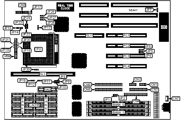
32-bit PCI slots (4), floppy drive interface, green PC connector, IDE interfaces (2), parallel port, PS/2 mouse interface, serial ports (2), cache slot, VRM connector, MediaBus slot |
|
NPU Options |
None |
|
CONNECTIONS | |||
|
Purpose |
Location |
Purpose |
Location |
|
Serial port 1 |
CN1 |
Reset switch |
CN8 pins 9 & 10 |
|
Serial port 2 |
CN2 |
Power LED & keylock |
CN8 pins 11 - 15 |
|
Parallel port |
CN3 |
Speaker |
CN8 pins 17 - 20 |
|
Floppy drive interface |
CN4 |
IDE interface LED |
JP17 |
|
IDE interface 1 |
CN5 |
Chassis fan power |
JP30 |
|
IDE interface 2 |
CN6 |
32-bit PCI slots |
PC1 - PC4 |
|
PS/2 mouse interface |
CN7 |
MediaBus slot |
SL1 |
|
Turbo LED |
CN8 pins 2 & 3 |
Cache slot |
SL2 |
|
Green PC connector |
CN8 pins 4 & 5 |
VRM connector |
VRM |
|
USER CONFIGURABLE SETTINGS | |||
|
Function |
Label |
Position | |
|
» |
On board multi I/O enabled |
JP4 |
Pins 1 & 2 closed |
|
On board multi I/O disabled |
JP4 |
Pins 2 & 3 closed | |
|
» |
PS/2 mouse disabled |
JP7 |
Pins 2 & 3 closed |
|
PS/2 mouse enabled |
JP7 |
Pins 1 & 2 closed | |
|
» |
CMOS memory normal operation |
JP13 |
Open |
|
CMOS memory clear |
JP13 |
Closed | |
|
Note: If the multi I/O chip is a UM8669F, JP4 is not used. It is enabled or disabled through the BIOS. | |||
|
DRAM CONFIGURATION | ||
|
Size |
Bank 0 |
Bank 1 |
|
8MB |
(2) 1M x 32 |
None |
|
8MB |
None |
(2) 1M x 32 |
|
16MB |
(2) 2M x 32 |
None |
|
16MB |
None |
(2) 2M x 32 |
|
16MB |
(2) 1M x 32 |
(2) 1M x 32 |
|
24MB |
(2) 1M x 32 |
(2) 2M x 32 |
|
24MB |
(2) 2M x 32 |
(2) 1M x 32 |
|
32MB |
(2) 4M x 32 |
None |
|
32MB |
None |
(2) 4M x 32 |
|
32MB |
(2) 2M x 32 |
(2) 2M x 32 |
|
40MB |
(2) 1M x 32 |
(2) 4M x 32 |
|
40MB |
(2) 4M x 32 |
(2) 1M x 32 |
|
48MB |
(2) 2M x 32 |
(2) 4M x 32 |
|
48MB |
(2) 4M x 32 |
(2) 2M x 32 |
|
64MB |
(2) 8M x 32 |
None |
|
DRAM CONFIGURATION (CON’T) | ||
|
Size |
Bank 0 |
Bank 1 |
|
64MB |
None |
(2) 8M x 32 |
|
64MB |
(2) 4M x 32 |
(2) 4M x 32 |
|
72MB |
(2) 1M x 32 |
(2) 8M x 32 |
|
72MB |
(2) 8M x 32 |
(2) 1M x 32 |
|
80MB |
(2) 2M x 32 |
(2) 8M x 32 |
|
80MB |
(2) 8M x 32 |
(2) 2M x 32 |
|
96MB |
(2) 4M x 32 |
(2) 8M x 32 |
|
96MB |
(2) 8M x 32 |
(2) 4M x 32 |
|
128MB |
(2) 8M x 32 |
(2) 8M x 32 |
|
Note: Board accepts EDO memory. Board also accepts x 36 SIMMs. | ||
|
CACHE CONFIGURATION | ||||
|
Size |
Bank 0 |
Bank 1 |
TAG |
SL2 |
|
256KB (A) |
(4) 32K x 8 |
(4) 32K x 8 |
(1) 8K/16K/32K x 8 |
Not installed |
|
256KB (B) |
None |
None |
None |
256KB module Installed |
|
512KB (A) |
(4) 64K x 8 |
(4) 64K x 8 |
(1) 16K/32K x 8 |
Not installed |
|
512KB (B) |
None |
None |
None |
512KB module Installed |
|
CACHE CONFIGURATION | |
|
Type |
JP16 |
|
Asynchronous cache enabled |
Pins 1 & 2 closed |
|
Asynchronous cache disabled |
Pins 2 & 3 closed |
|
CACHE JUMPER CONFIGURATION | |
|
Size |
JP12 |
|
256KB (A) |
Pins 2 & 3 closed |
|
512KB (A) |
Pins 1 & 2 closed |
|
CACHE VOLTAGE CONFIGURATION | ||||
|
Voltage |
JP8 |
JP9 |
JP10 |
JP11 |
|
Mixed voltage |
Closed |
Closed |
Open |
Open |
|
3.3v |
Open |
Open |
Closed |
Closed |
|
CPU SPEED SELECTION | |||||||
|
CPU speed |
Clock speed |
Multiplier |
JP14 |
JP15 |
JP26 |
JP27 |
JP28 |
|
75MHz |
50MHz |
1.5x |
Open |
Open |
1 & 2 |
2 & 3 |
2 & 3 |
|
90MHz |
60MHz |
1.5x |
Open |
Open |
2 & 3 |
2 & 3 |
1 & 2 |
|
100MHz |
66MHz |
1.5x |
Open |
Open |
2 & 3 |
1 & 2 |
2 & 3 |
|
120MHz |
60MHz |
2x |
Open |
Closed |
2 & 3 |
2 & 3 |
1 & 2 |
|
133MHz |
66MHz |
2x |
Open |
Closed |
2 & 3 |
1 & 2 |
2 & 3 |
|
150MHz |
60MHz |
2.5x |
Closed |
Closed |
2 & 3 |
2 & 3 |
1 & 2 |
|
166MHz |
66MHz |
2.5x |
Closed |
Closed |
2 & 3 |
1 & 2 |
2 & 3 |
|
Note: Pins designated should be in the closed position. | |||||||
|
CPU VOLTAGE SELECTION | |||
|
Voltage |
JP22 |
JP23 |
JP24 |
|
3.3v (STD/VR) |
Closed |
Open |
Open |
|
3.4v - 3.6v (VRE) |
Open |
Closed |
Open |
|
CPU VOLTAGE SELECTION | ||||
|
Setting |
JP18 |
JP19 |
JP20 |
JP21 |
|
VRM not installed |
Closed |
Closed |
Closed |
Closed |
|
VRM installed |
Open |
Open |
Open |
Open |
|
SERIAL PORT 2 SELECTION | |||
|
Setting |
JP1 |
JP2 | |
| » |
Used as COM2 |
Pins 1 & 2 closed |
Pins 1 & 2 closed |
|
FLASH BIOS SELECTION | ||
|
Setting |
JP5 |
JP6 |
|
Flash BIOS write protect enabled |
Pins 1 & 2 closed |
Pins 2 & 3 closed |
|
Flash BIOS write protect disabled |
Pins 2 & 3 closed |
Pins 2 & 3 closed |