APPARAT, INC.
AT COMBO CARD
|
Card Type |
Multi-I/O |
|
Chipset |
Unidentified |
|
Maximum Onboard Memory |
3MB DRAM |
|
I/O Options |
Parallel port, serial port |
|
Data Bus |
16-bit ISA |
|
CONNECTIONS | |||
|
Function |
Label |
Function |
Label |
|
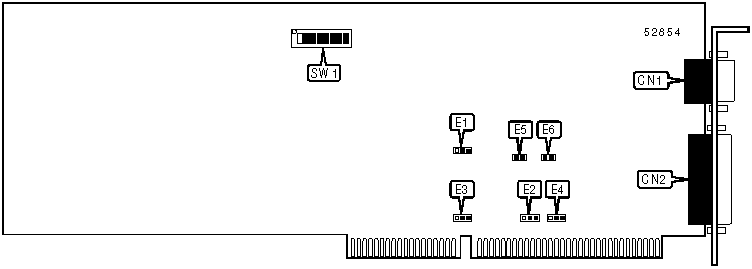
Serial port |
CN1 |
Parallel port |
CN2 |
|
USER CONFIGURABLE SETTINGS | ||
|
Setting |
Label |
Position |
|
Serial port address set to COM1: (3F8h) |
E1 |
Pins 2 & 3 closed |
|
Serial port address set to COM2: (2F8h) |
E1 |
Pins 1 & 2 closed |
|
Parallel port address set to 378h |
E3 |
Pins 2 & 3 closed |
|
Parallel port address set to 278h |
E3 |
Pins 1 & 2 closed |
|
Serial port enabled |
E5 |
Closed |
|
Serial port disabled |
E5 |
Open |
|
Parallel port enabled |
E6 |
Closed |
|
Parallel port disabled |
E6 |
Open |
|
Note:Disabling a port does not disable its respective interrupt; this must be done with the interrupt setting jumpers. | ||
|
STARTING MEMORY ADDRESS SELECTION | |||
|
Setting |
System Board Memory |
SW1/1 |
SW1/2 |
|
256KB |
256KB |
On |
On |
|
512KB |
512KB |
On |
Off |
|
1024KB |
640KB |
Off |
On |
|
1408KB |
1MB |
Off |
Off |
|
DRAM CONFIGURATION | ||||||
|
Starting Address Setting |
Bank 0 |
Bank 1 |
Bank 2 |
Bank 3 |
Bank 4 |
Bank 5 |
|
256KB |
(18) 256K x 1 |
None |
None |
None |
None |
None |
|
256KB |
(18) 256K x 1 |
(18) 256K x 1 |
None |
None |
None |
None |
|
256KB |
(18) 256K x 1 |
(18) 256K x 1 |
(18) 256K x 1 |
None |
None |
None |
|
256KB |
(18) 256K x 1 |
(18) 256K x 1 |
(18) 256K x 1 |
(18) 256K x 1 |
None |
None |
|
256KB |
(18) 256K x 1 |
(18) 256K x 1 |
(18) 256K x 1 |
(18) 256K x 1 |
(18) 256K x 1 |
None |
|
256KB |
(18) 256K x 1 |
(18) 256K x 1 |
(18) 256K x 1 |
(18) 256K x 1 |
(18) 256K x 1 |
(18) 256K x 1 |
|
512KB |
(18) 64K x 1 |
None |
None |
None |
None |
None |
|
512KB |
(18) 64K x 1 |
(18) 256K x 1 |
None |
None |
None |
None |
|
512KB |
(18) 64K x 1 |
(18) 256K x 1 |
(18) 256K x 1 |
None |
None |
None |
|
512KB |
(18) 64K x 1 |
(18) 256K x 1 |
(18) 256K x 1 |
(18) 256K x 1 |
None |
None |
|
512KB |
(18) 64K x 1 |
(18) 256K x 1 |
(18) 256K x 1 |
(18) 256K x 1 |
(18) 256K x 1 |
None |
|
512KB |
(18) 64K x 1 |
(18) 256K x 1 |
(18) 256K x 1 |
(18) 256K x 1 |
(18) 256K x 1 |
(18) 256K x 1 |
|
1024KB |
(18) 256K x 1 |
(18) 256K x 1 |
None |
None |
None |
None |
|
1024KB |
(18) 256K x 1 |
(18) 256K x 1 |
(18) 256K x 1 |
None |
None |
None |
|
1024KB |
(18) 256K x 1 |
(18) 256K x 1 |
(18) 256K x 1 |
(18) 256K x 1 |
None |
None |
|
1024KB |
(18) 256K x 1 |
(18) 256K x 1 |
(18) 256K x 1 |
(18) 256K x 1 |
(18) 256K x 1 |
None |
|
1024KB |
(18) 256K x 1 |
(18) 256K x 1 |
(18) 256K x 1 |
(18) 256K x 1 |
(18) 256K x 1 |
(18) 256K x 1 |
|
1408KB |
(18) 256K x 1 |
(18) 256K x 1 |
None |
None |
None |
None |
|
1408KB |
(18) 256K x 1 |
(18) 256K x 1 |
(18) 256K x 1 |
None |
None |
None |
|
1408KB |
(18) 256K x 1 |
(18) 256K x 1 |
(18) 256K x 1 |
(18) 256K x 1 |
None |
None |
|
1408KB |
(18) 256K x 1 |
(18) 256K x 1 |
(18) 256K x 1 |
(18) 256K x 1 |
(18) 256K x 1 |
None |
|
1408KB |
(18) 256K x 1 |
(18) 256K x 1 |
(18) 256K x 1 |
(18) 256K x 1 |
(18) 256K x 1 |
(18) 256K x 1 |
|
Note:Bank 0 may be used for either base (conventional) or extended memory, but not both. Therefore, when the starting address is set to either 256KB or 512KB, Bank 0 is used to raise the base memory to 640KB. Any remaining memory in Bank 0 is ignored. | ||||||
|
DRAM SWITCH CONFIGURATION | ||||||
|
Number Banks Installed |
SW1/3 |
SW1/4 |
SW1/5 |
SW1/6 |
SW1/7 |
SW1/8 |
|
1 |
On |
Off |
Off |
Off |
Off |
Off |
|
2 |
On |
On |
Off |
Off |
Off |
Off |
|
3 |
On |
On |
On |
Off |
Off |
Off |
|
4 |
On |
On |
On |
On |
Off |
Off |
|
5 |
On |
On |
On |
On |
On |
Off |
|
6 |
On |
On |
On |
On |
On |
On |
|
Note:SW1/3 to SW1/8 enable Banks 0 through 5 respectively. Banks 3, 4, and 5 are located on a daughterboard. The locations of the memory and daughterboard headers are unidentified. | ||||||
|
SERIAL PORT INTERRUPT SELECTION | |
|
Setting |
E2 |
|
IRQ3 |
Pins 1 & 2 closed |
|
IRQ4 |
Pins 2 & 3 closed |
|
Disabled |
Open |
|
PARALLEL PORT INTERRUPT SELECTION | |
|
Setting |
E4 |
|
IRQ5 |
Pins 1 & 2 closed |
|
IRQ7 |
Pins 2 & 3 closed |
|
Disabled |
Open |
|
MISCELLANEOUS NOTES |
|
The banks on the AT Combo card must be completely populated before the daughterboard can be used. The daughterboard contains banks 3 through 5. |