ATC/UNITRON COMPUTERS & COMPUTER PARTS
EX3135
|
Data bus: |
32-bit VL-bus |
|
Size: |
Three-quarter length, full-height card |
|
Hard drive supported: |
Two IDE(AT) drives |
|
Floppy drives supported: |
Two 360KB, 720KB, 1.2MB, or 1.44MB drives |
|
CONNECTIONS | |
|
Function |
Location |
|
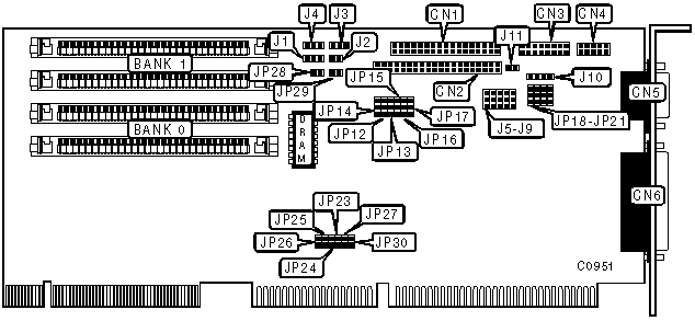
34-pin cable connector - floppy drive |
CN1 |
|
40-pin primary IDE(AT) connector |
CN2 |
|
16-pin game port |
CN3 |
|
10-pin serial port 2 - internal |
CN4 |
|
9-pin serial port 1 - external |
CN5 |
|
25-pin parallel port - external |
CN6 |
|
4-pin connector - drive active LED |
J10 |
|
USER CONFIGURABLE SETTINGS | |||
|
Function |
Location |
Setting | |
|
» |
Factory configured - do not alter |
J1 |
Pins 2 & 3 closed |
|
» |
Factory configured - do not alter |
J2 |
Closed |
|
» |
Factory configured - do not alter |
J3 |
Closed |
|
» |
IDE(AT) interface enabled |
J4 |
Pins 1 & 2 closed |
|
|
IDE(AT) interface disabled |
J4 |
Pins 2 & 3 closed |
|
» |
IDE port address 034h, 038h, 03Ch select |
J7 |
Pins 1 & 2 closed |
|
|
IDE port address 0B4h, 0B8h, 0BCh select |
J7 |
Pins 2 & 3 closed |
|
» |
Factory configured - do not alter |
J8 |
Pins 2 & 3 closed |
|
» |
Factory configured - do not alter |
J9 |
Pins 1 & 2 closed |
|
USER CONFIGURABLE SETTINGS (CONTINUED) | |||
|
Function |
Location |
Setting | |
|
» |
Two IDE(AT) drives present |
J11 |
Open |
|
|
One IDE(AT) drive present |
J11 |
Closed |
|
» |
Parallel port enabled |
JP12 |
Pins 1 & 2 closed |
|
|
Parallel port disabled |
JP12 |
Pins 2 & 3 closed |
|
» |
Factory configured - do not alter |
JP13 |
Pins 2 & 3 closed |
|
» |
Factory configured - do not alter |
JP14 |
Pins 1 & 2 closed |
|
» |
Floppy drive interface enabled |
JP15 |
Pins 1 & 2 closed |
|
|
Floppy drive interface disabled |
JP15 |
Pins 2 & 3 closed |
|
» |
Parallel port is LPT1(378h) |
JP16 |
Pins 1 & 2 closed |
|
|
Parallel port is LPT2(278h) |
JP16 |
Pins 2 & 3 closed |
|
» |
Game port enabled |
JP17 |
Pins 1 & 2 closed |
|
|
Game port disabled |
JP17 |
Pins 2 & 3 closed |
|
» |
Parity check disabled |
JP27 |
Open |
|
|
Parity check enabled |
JP27 |
Closed |
|
» |
M/B Chipset is not ALI 1429 A/G |
JP30 |
Closed |
|
|
M/B Chipset is ALI 1429 A/G |
JP30 |
Open |
|
Note: Parity check can only be enabled when using SIMMs with parity bit. | |||
|
BIOS ADDRESS SELECTION | |||
|
Address |
JP23 |
JP24 | |
|
» |
C8000-CFFFFh |
Closed |
Closed |
|
|
D0000-D7FFFh |
Open |
Closed |
|
|
D8000-DFFFFh |
Closed |
Open |
|
|
E0000-E7FFFh |
Open |
Open |
|
INTERFACE MODE SELECTION | ||
|
Mode |
J5 |
J6 |
|
386SX |
Pins 1 & 2 closed |
Pins 1 & 2 closed |
|
386DX |
Pins 1 & 2 closed |
Pins 2 & 3 closed |
|
486 |
Pins 2 & 3 closed |
Pins 1 & 2 closed |
|
CACHE I/O PORT ADDRESS SELECTION | |||
|
Address |
JP25 |
JP26 | |
|
» |
130h & 134h |
Closed |
Closed |
|
|
230h & 234h |
Open |
Closed |
|
|
300h & 304h |
Closed |
Open |
|
|
330h & 334h |
Open |
Open |
|
SERIAL PORT ADDRESS SELECTION | |||||
|
PORT 1 |
PORT 2 |
JP18 |
JP19 |
JP20 |
JP21 |
|
COM1 |
COM2 |
1 & 2 |
1 & 2 |
1 & 2 |
1 & 2 |
|
COM1 |
COM4 |
1 & 2 |
1 & 2 |
1 & 2 |
2 & 3 |
|
COM1 |
Disabled |
1 & 2 |
1 & 2 |
2 & 3 |
N/A |
|
COM3 |
COM2 |
1 & 2 |
2 & 3 |
1 & 2 |
1 & 2 |
|
COM3 |
COM4 |
1 & 2 |
2 & 3 |
1 & 2 |
2 & 3 |
|
COM3 |
Disabled |
1 & 2 |
2 & 3 |
2 & 3 |
N/A |
|
Disabled |
COM2 |
2 & 3 |
N/A |
1 & 2 |
1 & 2 |
|
Disabled |
COM4 |
2 & 3 |
N/A |
1 & 2 |
2 & 3 |
|
Disabled |
Disabled |
2 & 3 |
N/A |
2 & 3 |
N/A |
|
DRAM JUMPER CONFIGURATION | ||
|
Size |
JP28 |
JP29 |
|
On-board DRAM enabled (256 x 16) |
Open |
Open |
|
On-board DRAM disabled |
Closed |
Closed |
|
Note: When enabling DRAM do not fill Bank 0 and leave jumper JP27 open. | ||
|
DRAM CONFIGURATION | |||
|
Size |
Bank 0 |
Bank 1 |
On-board DRAM |
|
512KB |
(2) 256 x 9 |
NONE |
NONE |
|
512KB |
NONE |
NONE |
(1) 256 x 16 |
|
1MB |
(2) 256 x 9 |
(2) 256 x 9 |
NONE |
|
2Mb |
(2) 1MB x 9 |
NONE |
NONE |
|
2.5MB |
(2) 1MB x 9 |
(2) 256 x9 |
NONE |
|
2.5MB |
NONE |
(2) 1MB x 9 |
(1) 256 x 16 |
|
4MB |
(2) 1MB x 9 |
(2) 1MB x 9 |
NONE |
|
8MB |
(2) 4MB x 9 |
NONE |
NONE |
|
8.5MB |
(2) 4MB x 9 |
(2) 256 x 9 |
NONE |
|
8.5MB |
NONE |
(2) 4MB x 9 |
(1) 256 x 16 |
|
10MB |
(2) 4MB x 9 |
(2) 1MB x 9 |
NONE |
|
16MB |
(2) 4MB x 9 |
(2) 4MB x 9 |
NONE |
|
Note: 0KB of memory is also a valid configuration. | |||